A Simple and Cost Effective Method for Making Hole Transport Layer (HTL) Materials for Organic Electronics

- 領域
- Advanced Materials
- Patent
- IP00437
Key Problem and Market Opportunity
- The Hole Transport Layer (HTL) provides electron mobility in organic lighting devices (OLED). PEDOT:PSS is conventionally an ideal HTL material for testing OLED performance because it is highly electro-conductive and transparent in the visible light spectrum. However, PEDOT:PSS has limited lifetime for production environment due to its acidic property and causes corrosion of the ITO anode.
- Therefore, our materials can be a replacement for achieving longer lifetime for organic electronic devices without compromising its performance.
Key Advantages of the Technology

- Low-temperature one-step solution-process method for synthesizing transition metal oxides (TMOs) for HTL
- Water-free process – enhance yield and lifetime
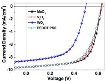
- Tested with multiple TMOs. For instance, molybdenum oxide (MoO3), vanadium oxide (V2O5) and tungsten oxide (WO3)
| MoO3 | V2O5 | WO3 | PEDOT:PSS | |
|---|---|---|---|---|
| Annealing temperature (10mins) | 80°C | 100°C | 100°C | 140°C |
| Open-circuit voltage for OSC (VOC) | 0.625 V | 0.625 V | 0.489 V | 0.633 V |
| Close-circuit current for OSC (JSC) (mA/cm2) | 9.38 | 9.71 | 8.60 | 9.28 |
| Fill Factor (FF) (%) | 67.15 | 63.61 | 56.48 | 62.69 |
| Power conversion efficiency | 3.94% | 3.86% | 2.37% | 3.68% |
Photovoltaic parameters for organic solar cells (OSC) with TMOs and PEDOT:PSS (approximate values)
Potential Product and Services
- Hole Transport Materials for Organic Electronics (HTL) such as OLED and organic solar cell
Development status and IP Strength
- US Patent no. 9540249
- Chinese Patent no. ZL 201380046404.8
- Broad protection for a wide selection of transition metal.
- Device prototype is available in laboratory scale