An Ultra-high Photoresponsive & Transparent Graphene Hybrid Phototransistor for Optoelectronic Applications
- 領域
- Electronics
- Patent
- IP00628
Key Problem and Market Opportunity
- Graphene is identified as a promising new material for making next-generation optoelectronic devices because of its flexibility, transparency, high carrier mobility, wavelength selectivity, gapless band structure and electronically tunable capability
- However, for phototransistor application, graphene phototransistors are suffering from low photoreponsitivity (< 1AW-1)
- The associating nano-fabrication process for existing graphene phototransistor is also expensive
Key Advantages of the Technology
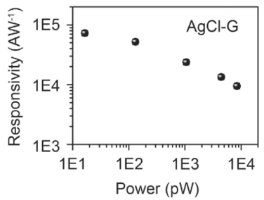
- HKU’s graphene hybrid phototransistor achieves an ultra-high sub-bandgap photoresponsivity of > 70,000AW-1
- Photoresponsiveness is within the visible range of 300nm to 700nm (13.6% effective EQE at 425nm)
- Spectral selectivity of the graphene hybrid phtototransistors may be tuned by controlling the thickness of the dielectric layer
- Photoabsorption properties can also be tuned by chemical modification or dye sensitization
- HKU’s graphene hybrid phototransistor is highly transparent and flexible
- Simple and low-cost fabrication process
| Prior Arts | HKU Graphene Hybrid Phototransistors | |
|---|---|---|
| Photoresponsivity | ✗ Low (< 1AW-1) | ✓ Ultra-high (> 70,000 AW-1) |
| Fabrication Process | ✗ Expensive | ✓ Low-Cost |
| Wavelength Selectivity Tuning | ✗ Complex | ✓ Simple |
Potential Product and Services
- Interactive Flat Panel Displays with embedded image detection for both touch and touch-free operations
- Flexible and wearable optoelectronic devices like Image Sensors, Biomedical Sensors and Optical Communication Sensors
Development Status and IP Strength
- US Patent Application No. 15/614,975
- Chinese Patent Application No. 201710426252.4
- Device prototype is available in laboratory scale


